Vias and trace resistance
Does vias in a trace affect the resistance (and the current carrying capability)? If so - does it get worse or better?
TL;DR - 5 mil traces gets a bit lower resistance with vias, thicker traces get ever so slightly worse.
Background
Back in September I asked this question on Twitter and it got a number of conflicting opinions. My personal thought was that it would get worse. But to really know I made a simple PCB to test a number of different versions and widths of traces with vias.
Of course this is just for one particular fab (JLCPCB) and just for a couple of traces, so no definite conclusions can be made but at least it points towards an answer.
The PCB I made have five traces each at 5,20 and 40mil (0.12, 0.5 and 1mm). The traces are all 100mm (about 4 inches) in length. Since I wanted to keep the PCB size within the limitations of the cheapest boards I had to meander them a bit, but that should not affect the result more than just a really tiny bit.
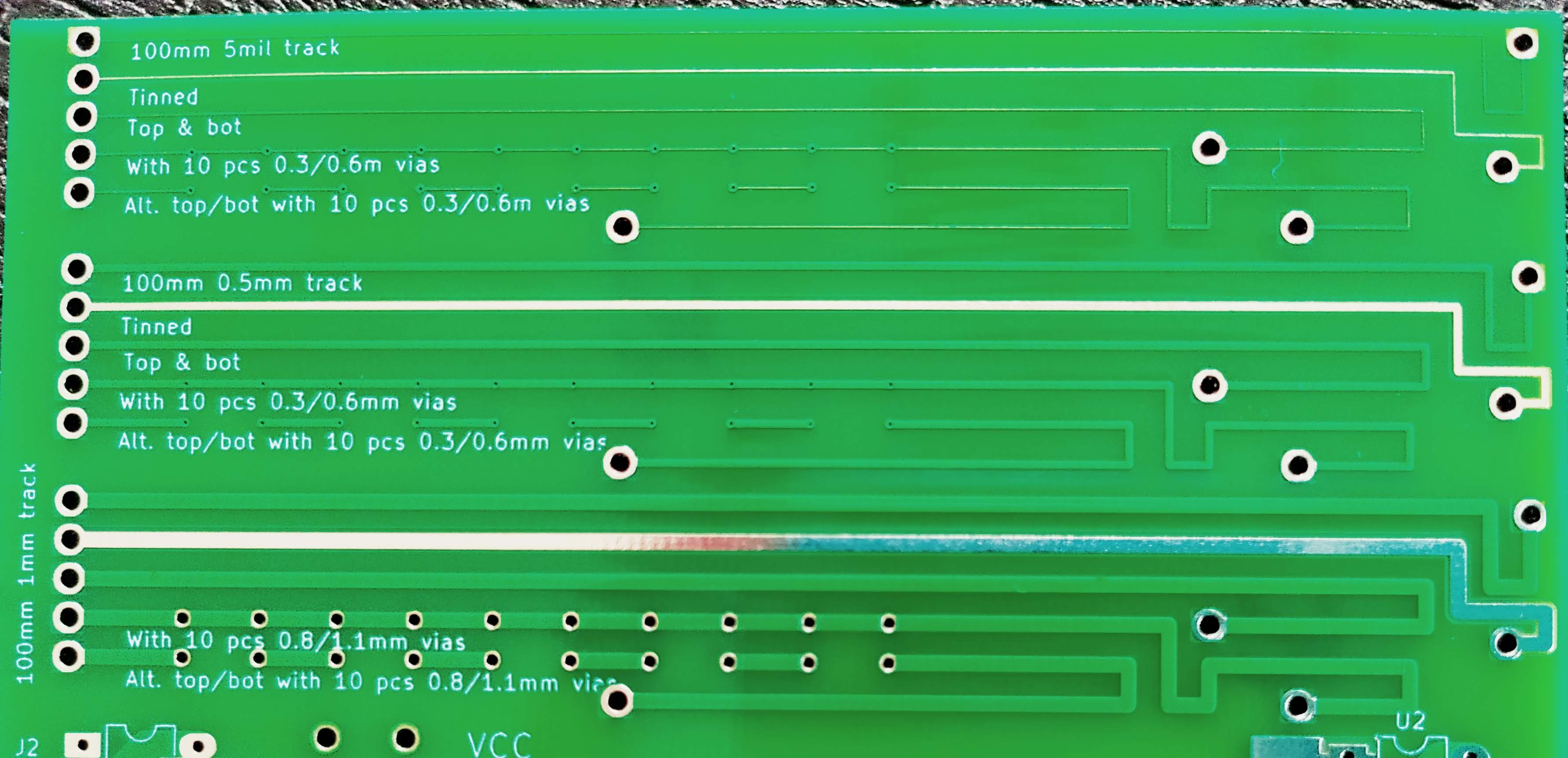
Traces
The first trace is just a plain trace to get a base reading.
The second trace have the solder mask removed to see if the thin layer of tin put there by the HASL process reduces the resistance.
The third trace have a trace on both bottom and top which should give roughly half the resistance.
The fourth trace have 10 vias inserted along the path. The vias aren’t connected at the bottom.
The fifth trace also have 10 vias but here the trace jumps to the other side of the PCB and contunites there until the next via.
Trace groups
The first group have 5 mil traces and the vias are 0.3mm with an annular ring of 0.15mm giving a total pad size of 0.3+0.15+0.15=0.6mm That’s the minimum sizes for their cheapest standard 2-Layer prototype boards. Ah yes, the boards have the regular 1oz copper as well.
The second group with the 0.5mm (20mil) traces have the same 0.3/0.6mm vias.
The third group with the beefier 1mm (40mil) traces have 0.8mm vias with the same 0.15mm annular rings giving s total of 1.1mm pad diameter.
Measurements
I made the measurements with my Keithley 197 microvolt 5 1/2 digit DMM using 4-wire Kelvin leads. In the 200 ohm range it gives me a 1 mOhm resolution. Maybe not super great, but probably enough for these simple measurements.
| 5 mil | Δ | 0.5 mm | Δ | 1 mm | Δ | |||
|---|---|---|---|---|---|---|---|---|
| Normal | 454 mΩ | ref | 78 mΩ | ref | 38 mΩ | ref | ||
| Bare | 437 mΩ | -4% | 80 mΩ | +3% | 39 mΩ | +3% | ||
| Double | 208 mΩ | -54% | 39 mΩ | -50% | 20 mΩ | -47% | ||
| Vias | 339 mΩ | -25% | 78 mΩ | 0% | 39 mΩ | +3% | ||
| Jumping | 410 mΩ | -10% | 89 mΩ | +14% | 41 mΩ | +8% |
Conclusions
The 25% reduction in resistace when the vias was put in the 5 mil trace clearly shows that the annular ring and part of the via-“tube” have a larger area than just the trace itself. (I didn’t expect that at all!)
The alterate top/bottom jumping was not as good as just having vias - that suggests that the via-tube do have a smaller cross section area compared to the trace.
The thicker (0.5 and 1 mm) traces got worse when broken up by vias, so for power traces it might be a good idea to put the vias just next to the main trace and have a short trace going between them. But the it’s only a couple of percent worse so maybe it really dosen’t matter. Maybe a proportionally larger annular ring would fix the issu as well.
Bare vs Normal
I don’t have an explanation for the bare trace having a slighly higher resistance compared to the covered 5 mil trace. It might just be a fluke. The thicker traces got slightly better, I guess the HASL process leave a very thin layer of tin on the trace so it doesn’t make much of a difference. S there’s no real use for doing this.
Just to check I manually added extra solder onto the bare traces. This got me a -8% (from the normal reference value) on the 5 mil,-16% on the 0.5 mm and -28% on the 1 mm trace. A 20-30% decrease in resistace is not bad and absolutely is something to consider for higher currents when you can’t widen the trace or don’t want to pay extra for 2oz copper.